La storia del transistor e la legge di Moore: evoluzione e architetture 3D
Slide da Fondamenti di Elettronica sulla storia del transistor e la legge di Moore. Il Pdf, adatto a studenti universitari di Fisica, esplora l'evoluzione tecnologica del transistor, i progressi nei materiali e le architetture 3D come FinFET e Gate All Around.
Mostra di più18 pagine


Visualizza gratis il Pdf completo
Registrati per accedere all’intero documento e trasformarlo con l’AI.
Anteprima
Corso di Fondamenti di Elettronica
La storia del transistor e la legge di Moore
prof. S. GerardinTransistor: from Conception to First Demonstration
- 1928-1935: first conception by Julius Lilienfeld "If electrons are
already in any solid and they can be moved around in a
controlled way, why are we extracting them (via a heated
filament), manipulating them via a grid and finally collecting
them again at the anode?" - 1930: patent by Lilienfeld, "Method and apparatus for
controlling electric current" described the first FET-like device - 1935: patent by Oskar Heil, first MOSFET
- 1945: patent by Shockley showing a device with a source,
gate, and a drain region, with flow of charge from S to D
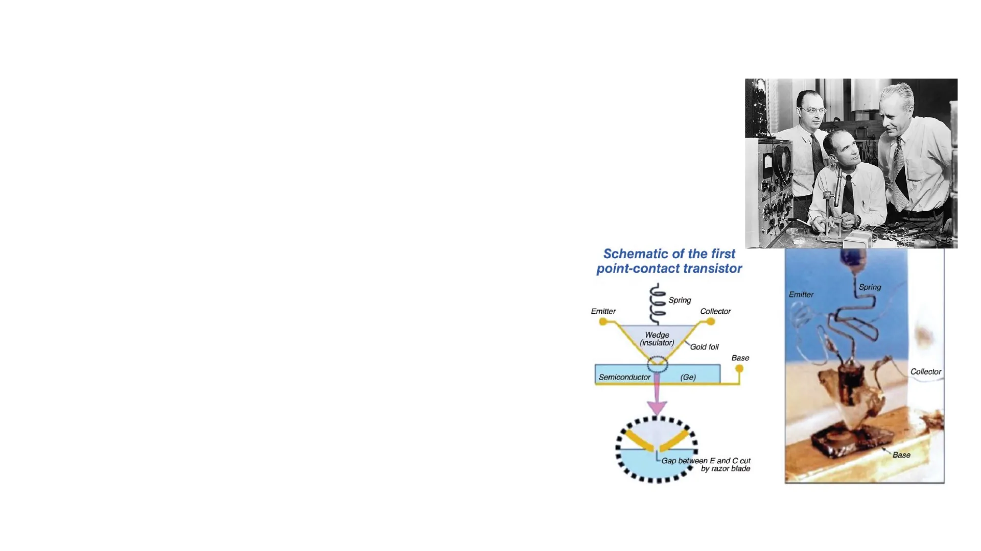
controlled by G voltage - 1947: experimental demonstration of first transistor (Ge) by
Bardeen and Brattain - 1956: Nobel prize to Bardeen, Shockley, Brattain for the
invention of transistor. Shockley moved to Palo Alto, CA, US
and started Shockley Semiconductor Lab
John Bardeen,
William Shockley,
Walter Brattain.
Publicity picture
produced by Bell
Labs at the time of
the announcement
(June 30, 1948)
Schematic of the first point-contact transistor
Spring
Emitter
Collector
Wedge
(insulator)
Gold foil
Base
Collector
Semiconductor
(Ge)
Base
Gap between E and C cut
by razor blade
1st transistor (Bell Lab, 1947): A plastic wedge secured two gold
contacts to Ge surface. Voltage applied to one contact
modulated the current flowing through the other
Spring
EmitterTransistor: Implementation
- 1957: "traitorous eight" left Shockley Semiconductor
Lab for the difficult relation with Shockley and
founded Fairchild Semiconductor, which then
became an incubator of Silicon Valley, being involved
in the creation of several corporations, e.g. Intel,
AMD (aka "Fairchildren": more than 40 companies
had been created by 1972!) - 1959: Mohamed Atalla & Dawon Kahng developed
the MOS transistor with SiO2 and Al metal gate. New
method for semiconductor device fabrication:
thermal growth of silicon oxide on Si substrate by
thermal treatment in oxidizing atmosphere (not
deposition). This process then enabled the mass-
production of silicon integrated circuits
"Traitorous eight" (including Gordon Moore
on the left and Robert Noyce 4th from the left)
Mohamed Atalla and Dawon Kahng, Bell LabsTransistor: Diffusion
- 1960: first planar transistor sold (bipolar)
- 1960: first MOS, 20 um, oxide thickness
~150 nm (passivation method solved issue
of surface interface states), Al gate - 1965: Moore's law
- 1968: first IC with polysilicon gate (F.
Faggin, Fairchild Semiconductor) - 1968: Noyce and Moore founded Intel
- 1971: first microprocessor - Intel 4004
100
Relative Manufacturing Can't por Component
962
1965
102-
1970
10
1
1
10
10 ª
104.
TO5
Number of Components per Integrated Carcent
Moore's Law
Announcing
a new era
of integrated
electronics
4001
4002
14003
A micro-
programmable
computer
on a chip!
-----
---------
F.
4004
Federico Faggin
Intel 4004 Microprocessor
intel
delivers.Moore's Prediction
Benefits of miniaturization
(more features, faster
circuits)
Technological
costs/difficulties for
fabrication of more
complex components
- Gordon Moore (1965): «The complexity
for minimum component costs has
increased at a rate of roughly a factor of
two per year. Certainly over the short
term this rate can be expected to
continue, if not to increase. Over the
longer term, the rate of increase is a bit
more uncertain, although there is no
reason to believe it will not remain nearly
constant for at least 10 years» ->br>exponential growth! - Observation of reality/forecast based on
economic principles
Relative Manufacturing Can't por Component
12
11
1965
10
9
8
7
102
1970
6
5
10
3
2
1
1
1
10
70%
10ª
104 105
Number of Components per integrated Carcent
1959
1960
1961
1962
1963
1964
1965
1966
1967
1968
1969
1970
1971
1972
1973
1974
1975
YEAR
TT
5
COMPONENTS PER INTEGRATED FUNCTION
/
15
14
13
962
LOG OF THE NUMBER OF
16
-
G.E. Moore, "Cramming more components onto integrated circuits," Electronics, 1965Moore's Law
- Moore's prediction published in 1965
had become a verified reality by 1975 - In 1975 Moore's prediction was
officially named Moore's Law "The
transistor growth rate was going to
reduce to doubling every 2 years in the
foreseeable future" - Moore's law guided the technology
evolution of digital systems in recent
decades, pushing the industry to align
with its predictions (self-fulfilling
prophecy)
1 M
2x/2Year
O BIPOLAR LOGIC
BIPOLAR ARRAYS
MOS LOGIC
64 K
MOS ARRAYS
.
COMPONENTS PER CHIP
4 K
256
2x/Year
16
10
60
65
70
75
80
YEAR
G. Moore, IEEE International Electron Devices Meeting, 197550 Years of Evolution in Microprocessors
107
106
105
Single-Thread
Performance
(SpecINT x 103)
104
Frequency (MHz)
103
102
Typical Power
(Watts)
101
Number of
Logical Cores
100
.
-
1970
1980
1990
2000
2010
2020
Transistors
(thousands)
Data collected by M. Horowitz, F. Labonte,
O. Shacham, K. Oukotun, L. Hammond,
C. Batten, K. Rupp
1960s-1970s:
Mainframe
computers (business,
scientific applications)
1980's-1990's:
Personal computer
(general purpose,
gaming)
2000's:
Server for
network
applications
2010's - Today: Mobile phones,
telecommunications/video streaming devices,
high performance platforms for IoT, cloud, AI,
virtual reality, autonomous vehicles, ...Understanding the Scale of Moore's Law
- The rate of innovation predicted (and actually
realized) by Moore's Law is unprecedented in
all human fields! - Automotive: if car mileage was scaled at the same
rate, a car today could drive the equivalent
distance between the Earth and the Sun with a
single gallon of gas - Agriculture: if productivity evolved at the same
rate, today we could feed the whole planet on a
square kilometer of land - Space travel: if the speed evolved at same rate,
today we could be travelling at 300 times the
speed of light
Stacy Smith, VP Intel, March 2017Until End of '90's: Scaling, Scaling, Scaling
- It was possible to follow Moore's law by
scaling device physical dimensions - Miniaturization lead to improved functions
and performance of ICs
1971: Intel 4004
10 um
2 000 transistors
1978: Intel 8085
3 um
1989: Intel i486
1 pm
1999: Intel Pentium III
250 nm
2000: Intel Pentium 4
180 nm
Generation
N
Generation
N+1
Generation
N+2
Generation
N+3
2003: Intel Centrino
130 nm
100 000 000 transistors
Credit: IntelPredictions on Gate Oxide Scaling
You Are Herel
4
Tox equivalent (nm)
3
1999
2
2001
Gate
1.2nm SIO
1
2003
109753
Silicon substrate
2005
0
4
8
12
1997 NTRS
Monolayers
1997 National Technology Roadmap for SemiconductorsNot only Scaling
Sidewall
Source
Gate
Drain
Channel
Active silicon
Buried
oxide
-
SiGe
SiGe
Substrate
1989: Silicon On
Insulator (SOI)
High-k
SiGe
SiGe
2003: Strained
Silicon
Silicon
2007: High-K, Metal
gate
2010: FinFET
(22 nm)
TECHINSIGHTS
2012: Tri-gate
transistor
2014
2016: 3D integrated chip
(3D NAND Flash memory)
· Scaling and ...
· New materials
· New device architectures
· New manufacturing techniques
MetalNew Materials
H
He
H
He
Li
Be
B
C
N
O
F
Ne
Na
Mg
Al
Si
P
S
Cl
Ar
K
Ca
Sc
T
V
Cr
Mn
Fe
Co
Ni
Cu
Zn
Ga
Ge
As
Se
Br
Kr
Rb
Sr
Y
Zr
Nb
Mo
Tc
Ru
RI
Pd
Ag
Cd
In
Sn
Sb
Te
I
Xe
Cs
La
Hf
Ta
W
Re
Os
Ir
Pt
Au
Hg
Tl
Pb
Bi
Po
At
Rn
Fr
Ra
Ac
Rf
Db
Sg
Bh
Hs
Mt
Ds
Ce
Pr
Nd
Pm
Sm
Eu
Gd
Tb
Dy
Ho
Er
Tm
Yb
Lu
Th
Pa
U
Np
Pu
Am
Cm
Bk
Cf
Es
Fm
Md
No
Lr
. The variety of materials needed by the electronics industry is now
much greater than a few decades ago
. Silicon: from Silicon to strained Si (2003) to increase carriers' mobility
· High-k (2007): from thin oxides to thicker oxides having the same performances
. Interconnections: from Aluminum to Copper
· Geopolitical problems
M. Bohr, ISSCC 2009
Metal
High-k
SiGe
SiGe
Silicon
Core 2 Duo Intel 45-nm (strained
Si, high-k gate oxide, metal gate)
Li
Be
B
C
N
O
F
Ne
Na
Mg
A
Si
P
S
Cl
Ar
K
Sc
Ti
V
Cr
Mn
Fe
Co
Ni
Cu
Zn
Ga
Ge
As
Se
Br
Kr
Rb
Sr
Y
Zr
Nb
Mo
To
Ru
Rh
Pd
Ag
Cd
In
Sn
Sb
Te
I
Xe
Cs
Ba
La
Hf
Ta
W
Re
Os
Ir
Pt
Au
Hg
Pb
B
Po
At
Rn
Fr
Ra
Ac
Rf
Db
Sg
Bh
Hs
Mt
Ds
Ce
Pr
Nd
Pm
Sm
Eu
Gd
Tb
Dy
Ho
Er
Tm
Yb
Lu
Th
Pa
U
Np
Pu
Am
Cm
Bk
Cf
Es
Fm
Md
No
Lr
Materials
< 1990
Materials
today
Ca
BaNew Architectures: 3D
- Today, the miniaturization of transistors has to cope
with the physical limits of matter - Insulations (e.g. gate oxide) cannot go below the
thickness of an atomic layer! - Greater and greater challenges (process, cost, ... )
- Traditionally, electronic chips are planar (e.g.
transistors are arranged on a single surface) but, to
progress further, more modern technologies expand
into the third dimension - 3D Transistor
- FinFET (2010)
- Gate All Around (GAA) (2022)
- Nanowire, nanosheet
- Superior performance because the signal control takes
place by completely surrounding the passage channel,
and not from only one side as in planar transistors
DRAIN
GATE
FIN
SOURCE
FinFET
GATE
DRAIN
SOURCE
Transistor GAACMOS Scaling: History and Roadmap
1000
You are here
250
Planar
180
130
90
100
65
-Old feature size
O
32
45.
22
FDSOI
....... ITRS Node name
16/14
10
...
... IRDS Node name
10
FinFET
5
3
GAAFET
2
1.5
0.7
1
0.5
0.1
1990
1995
2000
2005
2010
2015
2020
2025
2030
2035
Year of production ramp-up
[ITRS report, 2007-2013 editions]
[IEEE IRDS report, 2016-2022 editions]
V. Pouget, Short Course RADECS 2023
Nanometers
1NAND Flash: First Example of 3D Chip
Z
2D NAND
3D NAND
. 3D memories with more and more layers
of cells stacked on top of each other
(today > 200!), increasing the total
number of bits
2D NAND 16 nm
3D NAND 13 nm
176
160
Number of cell layers
128
96
96
764
48
32
24
16
2014
2015
2016
2017
2018
2019
2020
2021
Year
Credit: MicronWhat's Next?
3.5
3
Equivalent Node [nm]
2.5
2
1.5
1
0.5
0
2020 2022 2024 2026 2028 2030 2032 2034 2036 2038
Year
International Roadmap for Devices and Systems, 2022
· 2022: IRDS predicts a continue decrease in
transistor size
· More Moore: new architectures, technologies, materials
. More than Moore: integration of heterogeneous
technologies, functional diversification, etc.
· Challenges: process complexity, power dissipation issues
Top S/D
Gate
Gate
Bottom S/D
Vertical Transport Field
Effect Transistor (VTFET)
H. Jagannathan, et al., IEDM 2021
Stacked FET
J. Wang et al, VLSI 2021
Non hai trovato quello che cercavi?
Esplora altri argomenti nella Algor library o crea direttamente i tuoi materiali con l’AI.
